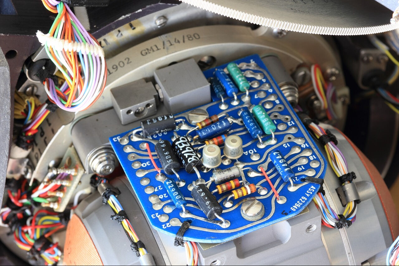
As an electronic equipment manufacturer committed to sustainable development, Mailin Electronic Technology focuses on using environmentally friendly materials and processes to provide professional PCBA board manufacturing services for precision electronic equipment such as audio amplifiers. Our green solder mask spray surface treatment technology not only improves the durability and reliability of the product, but also reduces the impact on the environment during the production process, reflecting our commitment to environmental protection. The green solder mask spray surface treatment technology provides a uniform and smooth protective layer for our PCBA products, which not only enhances the mechanical strength of the solder joints, but also improves the resistance to moisture and oxidation, ensuring that the audio amplifier operates in various Maintain optimal performance under ambient conditions. In addition, this surface treatment technology also simplifies later repairs and replacement of components, improving the maintainability of the product.
Our quality control process strictly follows international standards. From the screening of raw materials to the testing of final products, every link is carefully inspected and verified. Our goal is to ensure that each PCBA board meets the high standards of audio equipment and provides customers with a clear, pure sound quality experience.
In short, our professional green solder mask spray surface integrated circuit audio amplification PCBA board manufacturing service combines environmental protection concepts and advanced technology, aiming to provide customers with high-quality, high-performance audio electronic equipment. We are committed to advancing the development of audio technology and providing superior electronic products to customers around the world through continuous innovation and improvement.


|
SMT project
|
Sample(less than 20pcs)
|
Small and medium batch
|
||||
|
Maximum card board
|
No size limit
|
L50*W50mm-L510*460mm
|
||||
|
maximum plank
|
No size limit
|
3mm
|
||||
|
minimum plank
|
No size limit
|
0.2mm
|
||||
|
Minimum chip component
|
01005 package and above
|
150mm*150mm
|
||||
|
Maximum chip component
|
No size limit
|
Maximum component placement accuracy 100FP
|
||||
|
Minimum lead part spacing
|
0.3mm
|
0.3mm
|
||||
|
SMT capability
|
50-100 models
|
3-4 million points/day
|
||||
|
DIP plug-in capabilities
|
100,000 points/day
|
|||||


Our friendly team would love to hear from you!