
 EN
EN


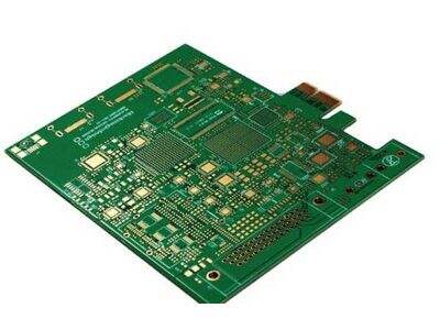
It requires a lot of effort to build custom projects, and there are many crucial components to consider. Developing a Printed Circuit Board (PCB) is one of those critical components. PCB is a flat board with lines, metal parts and holes. You use these parts to connect the electronic pieces together so you can build a project that can actually work and do what you want your project to do.
The very first thing you need to do to make a PCB is to design the circuit with a computer program. This design indicates how all the various elements of the project will be linked up. Once your die is complete, you print to special sheet plastic with copper on one side. The sheet this is placed on is known as its substrate. The copper regions of the substrate become the lines, or traces, that link the various areas of the circuit. We call that spaces, or gaps, in the control lines the areas in the board that do not conduct electricity, significant and to ensure the functional of circuit.
Once the design is printed onto the pcba circuit board substrate, its time to treat the printed circuit board to blast away all unnecessary copper. Etching is the process that does this. This process of removing unwanted copper leaves tiny holes throughout the board in strategic locations to enable connections between parts. A solder mask is then applied, a special layer. This layer serves as a protective barrier for the board traces, helping to prevent issues such as short circuits, which can occur if the electricity flows into the wrong direction. Last, silk-screening prints important info about the board and its components directly onto the board.
Considerations for Deciding the Method for PCB Fabrication
There are tons of factors to take into account while deciding on how should you make your PCB. One key reason the for complexity of your project. If you have a lot of complexity in your project, it could also mean that you need more advanced PCB fabrication methods to make sure everything functions correctly. I mean, simpler projects might work best with less complicated methods.
is the quality of the materials that you would be using to manufacture the PCB. So yes, using quality materials can make your pcb board more durable and reliable, too. That means when you eventually run it, it is less prone to have issues or break. You also want to think about how big a board you need and how many layers it will be. Because separate projects may need thicker boards with multiple layers or single layers.
Old Vs New PCB Making Methods: How to Choose
There are a few different PCB making techniques out there, but generally fall into one of two major categories: old methods and new methods. Old techniques involve more human work and effort and new techniques apply machines and automation for the fast and easy process.
Old methods include hand-drawing designs, using drill presses to make holes, and chemical etching to remove unwanted copper. Although they may require much time and work, these techniques can also be much more affordable for simple tasks. But they do not always lead to perfectly consistent outcomes, with potentially serious consequences.
On the contrary, new approaches are generally much more automatic. They are meant to be quicker, more energy efficient, and more accurate. These methods utilize computer-aided design (CAD) software to produce the circuit designs, while automated etching machines and laser drilling do the rest. While these modern technologies are more expensive on the front end, they will often lead to much higher quality PCBs, produced far faster and with far fewer errors, thus saving money on downstream processes.
How to Get Your Custom PCB Projects Right: New Trends in PCB Making
New trends constantly emerge because of the continuously changing nature of PCB manufacturing. A significant advancement in this domain is the introduction of flexible PCBs. These unique PCBs are designed to bend and twist without shattering, so work really well in wearable tech and medical devices. Flexible pcb are much more versatile as they can be bent to fit tight spaces and into different shapes based on its applications that makes it extremely handy with modern technology.
Using smaller components, such as surface-mount devices (SMDs), is another positive trend. These elements are smaller, lighter than conventional electronic components. Minimizing the size in this way can contribute to the overall board being smaller, one of many important criteria in many designs. Moreover, the usage of small components can enhance the performance of the PCB, so a PCB can operate efficiently for an extensive period of time without any difficulty.
How to Make More Intelligent Decisions in PCB Making
Selecting the most relevant method of creating a PCB for your custom project is a decision that needs to be thoroughly considered. Understanding the basics of how PCBs are made and considering what factors matter in a good fabrication process as well as the tradeoffs between older and newer techniques will help you to ensure that your project is successful and meets your needs.
